AUTOMATIXARON
FPGA as hardware accelerator
Aim of the tutorial:
In this tutorial, we will design a communication module to interface a hard processor.
Prerequisites:
Previous FPGA tutorials, some knowledge of serial communication protocols, Arduino IDE
Tutorial structure:
This one will be a lengthier tutorial, so here is a structure of sorts, with a small description.
-
Introduction into hardware accelerators - here we will look at the universal realization of hardware acceleration by combining the hardcore processor with general or dedicated peripherals (theory).
-
Simple serial protocol implementation - here we will implement a soft SPI slave core which accumulates the received data into an 8b RX register, and sends the bits of an 8b TX register to the master (theory, simulation, implementation).
-
8b RAW to register interface - here we will create a finite state machine with data path, to combine the 8b RX/TX values into command signals, R/W (read/write) registers, and RO (Read-Only) registers (theory, simulation, implementation).
1. Hardware accelerators:
Hardware acceleration is a specialized component which can perform an algorithm more efficiently than a general-purpose processor. We can implement any algorithm in a general processor, while the hardware accelerators are up for only specific tasks. Here we can consider a GPU/CPU interaction in case of computer graphics (e.g. ray-tracing), and teaching neural networks; DSP cores for efficient FFT and filter implementations; Cryptographic accelerators, Compressing accelerators etc.
A sorting algorithm would be a perfect example for an algorithm which runs more efficiently on a general-purpose processor, than specialized hardware.
Specialized connections enable the communication between processors and accelerators: in the case of GPU, there is the PCI-ex x16 bus, for example. In the case of simple architectures, there is the Wish-Bone bus, AMBA (e.g. AXI4). These are all parallel buses designed for optimal/fast data transactions.
We will pair an FPGA with an Arduino board, and implement a serial communication protocol between them because of hardware constraints. The trade-off of the simple bus is hardware complexity and speed reduction. We could consider a few options if we would want to send data to two 32b wide data registers, one 8b wide control register, and we would also want to read from a 32b wide data register:
-
A 32b wide data I/O line, and 2b wide address line (with CLK and RW) - read and write in one cycle.
-
A 16b wide data I/O line, and 3b wide address line (with CLK and RW) - read and write in two cycles.
-
An 8b wide data I/O line, and 4b wide address line (with CLK, and RW) - read and write in four cycles.
-
separate 1b input, and output line (with CLK) - read and write in min. Eight cycles.
There could be other possibilities such as separating the I/O lines into In- and Out-lines, or adding data/instr flag line etc. but even in these few examples, the speed/complexity ratio is evident.
A few words about the SPI master: we will use an Arduino Nano as the master. I'm usually avoiding the Arduino environment as best as I can, because of reasons, but in this case, an Arduino board will suffice.
2. Simple serial protocol implementation:
We have chosen the SPI serial communication since, we have only one master (and one slave in this case), the communication speed can be as fast as 40Mbps, uses a common clock signal, and on the low level, the underlying implementation is a single FIFO register.

Here we can see a simple SPI master with three SPI slave devices. Each slave has a joint clock signal (SCLK), a joint input (MOSI, master out slave in), a joint output (MISO, master in slave out), and separate chip select (CS) or slave select (SS) lines. Only the active slave will read and write on the MOSI/MISO lines.
The SS/CS signal is always active low.
The SCK/SCLK can be active-low or active-high depending on the CPOL setting (0 or 1 respectively). CPOL = 0 means that the idle is 0, the leading edge is a rising edge, the trailing edge is a falling one.
CPHA determines the timing of the MOSI/MISO signals relative to the clock. CPHA = 0 means the out side changes the data on trailing, while the in side captures on leading-edge.

We use the terms Mode 0, 1, 2 or 3 when we are talking about an SPI protocol with CPOL = 0 / CPHA = 0, CPOL = 0 / CPHA = 1, CPOL = 1 / CPHA = 0, or CPOL = 1 / CPHA = 1 respectively.
In this tutorial, we will design the SPI communication with Mode 3.
We design the master first. I'm using Visual Studio Code with Platform IO IDE, but the Arduino IDE can also be used because the compiler is the same.
Here we use the default SPI pin configuration, with software-controlled CS pin.
We configure the UART and the SPI, and the output pins at the start of the program.
The LED pin is used to indicate the start and end of a transaction visually. We activate the slave by pulling the CS pin down. The Master clock speed is configured for 1MHz, and we use the Mode 3.
We transfer a number from 0 to 255 in each second, and we also display the received value on the serial port.
We saw that the master device generates the SCLK signal, sends the MOSI and expects the MISO signal synchronous to SCLK. The problem is that the slave device has its clock signal, so we need to re-sample and synchronise the incoming data to the system clock.
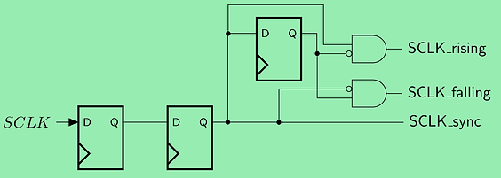
Here I've shown the synchronisation of the SCLK signal. Usually, a 2b wide register is enough for the purpose, but we need to check the rising and falling edges, for which we will be using the two upper bits.
We can see the implemented design, which generates the rising and falling edge signals from the synchronised SCLK line.
We can use the same implementation for the SS line to synchronize and to detect the edges.
We can implement the MOSI synchronisation with only two flip-flops since the edge detection is not required.
The slave internally generates the MISO data, so no synchronisation is necessary.
Operation logic: So far, we have the synchronized signals. The next step is to use an internal 8b storage register and implement the SPI mode3 protocol:
-
Transfer the MSB of the storage register to the MISO on the falling edge of SCLK...
-
Shift the MOSI data to the LSB position of the storage register on the rising edge of SCLK.
Lastly, we will strobe a flag (rx_valid) if we received 8b worth of data.

We can see the top module on the image to the right.
Let's set the internal oscillator frequency to 7MHz, and configure the PLL to output a clock signal with 280MHz frequency.
We can connect the SPI signals to our module.
We use a register to store the RX data when we get a rx_valid signal. We use this stored value in the next transfer cycle as TX data.
The figure below shows the expected simulation results so that we can upload the bit file to the device.

A strange phenomenon happens when we upload the JEDEC file. The Arduino sends an increasing data sequence from 0 to 255, but the slave sends back a somewhat non-deterministic data (increases randomly, jumps back, stops increasing).
The problem is the system clock. We can see some peculiar warnings if we take a look at the Place & Route Reports in Diamond. The IDE warns us that we requested a signal with f > 200MHz, but the signal integrity can only be guaranteed up to 120MHz, so let's do something about this.
We can change the PLL output frequency to 105MHz, and upload the newly generated JEDEC file. Now the warnings are gone, and the slave response is the previously sent data byte, as expected.
You can download the project files for the master and slave device from here.
3. SPI register interface
It would be nice if we could read from and write in 32b registers with our small SPI interface, but so far it is not possible. In this part of the tutorial, we will implement a message interface (16 total registers at maximum) with a status register.
Let the address of the status register be 0x00, the address range of the read registers between 0x80 and 0x8F, and the address range of the write registers between 0xC0 and 0xCF. Further down the line, we could expand the register state in the range of 0x01 - 0x0F (this is ideal for control options).
Every data exchange starts with the master sending the appropriate address value while ignoring the incoming data. In case of the status, the master sends a dummy byte and reads the actual value. The master sends 4 Bytes of dummy data and interprets the incoming values in the case of the reading operation. Lastly, the master sends the 32b TX data in four 1 Byte chunks.
In our implementation, we will have three registers, the first two are r/w, and the last one will be read-only. We will use this register scheme to implement the arithmetic core latter on (e.g. R3 = R1 + R2).
Let's have a few words about the SPI master.
We will similarly design the master to the previous implementation. The Arduino should print an options menu on the terminal: one for status check, two for write test, three read test, four flag test. The master goes into an infinite loop after printing the messages and waits for user input.
If we type 1, the master will send 0x00 and dummy data (0xFF). If the received value is 0x69 (the slave ID), the status check is successful.
If we type 2, the master will ask for the register number (0 or 1), then it will write data to the specific register (0xC0 or 0xC1), and it will read back the value from the register for checking. The write test is successful if the written ad read values are the same.
If we type 3, the master will read the value from the read-only register, and compare its value with the expected (0xDEADBEEF) constant. The read test is successful if the values are the same.
If we type 4, the master will send a start flag (0x01) which turns on an LED. Any consecutive data transaction should turn the LED off.
I will put the code of the Arduino master at the end of this section since that is not the main focus here.
We will write the hardware description in System Verilog because there we can use multi-dimensional arrays.
If we have the number of R/W and RO registers as parameters NR_RWREGS and NR_ROREGS, respectively, the overall register structure will be:
Otherwise, we would have to flatten the 2D register structure into a 1D register (the silicon won't mind, and the synthesiser will optimise the structure to fit the parameters, but it's more readable this way).

We will implement a finite state machine to parse and execute the received commands:
-
Idle state (0).
-
Transmit Status (TS) state (1): sends the slave ID to the master.
-
Start Flag (SF) state (2): sets a start flag register.
-
Transmit Register value (TR) state (3): sends the required register value.
-
Receive Register value (RR) state (4): receives a 32b value from master.
We saw in previous tutorials how to use the case instruction, but there are some wild varieties of the simple case - casez and casex, which we will use here.
casez - allows statements 'Z' and '?' to be treated as don't care: the statement 2'bZ0 can match 2'b00, 2'b10 and 2'bZ0, which is ideal for a priority decoder. The casez offers an elegant way for the if-else replacement.
casex - allows statements 'X', 'Z' and '?' to be treated as don't care values. 'X' values can propagate through design and will mask some design issues. These 'X' values can cause problems when they get into a casex problem, so the best practice is to omit the usage of casex. This means we will use it :).
All of the source files are located here. It shouldn't be hard to understand the hardware description of the slave if you've followed the tutorials.

In the simulation, we can see that the slave status is transferred successfully (the old status was 0x5A, the new one is 0x69). We can write into registers 0 and 1. We can read the stored message from the RO register (this is shown between transitions 14 - 17 of tx_wire, or in the MISO line for people keen on binary signals).
We can test the hardware setup after programming the Arduino with the given SPI master code, and after the download of the JEDEC file to the FPGA.
+1. Minimalist ADD/MUL accelerator
If you did arrive at this point, you could easily add custom IPs to the FPGA. The IP core will read the data from the R/W registers and will write the result to the RO register. Sending some start flag will initiate the operation, and the IP could generate external interrupts if necessary.
Now, of course, the IP must fit in the remaining space in the FPGA.
Here I will show how to design a simple arithmetic accelerator for unsigned integer addition and multiplication.
Here we use a case syntax to distinguish the addition from the multiplication. We extend the input numbers taking into consideration the sign of the numbers. Finally, we concatenate the result to match the output data width. We can see in the simulation, that the arithmetic core works as intended.

We can add the following commands to the master side program:
-
Send data to reg1 : -111
-
Send data to reg2: -1
-
Write OP1
-
Read reg3: ~ Here we should see -112 on the terminal (-111 + (-1) )
-
Write OP2
-
Read reg3: ~ Here we should see 111 on the terminal (-111 * (-1))